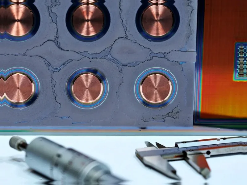
According to Nature, researchers have developed a chemical liquid deposition approach that transforms amorphous zeolitic imidazolate frameworks from empirical materials into predictable semiconductor resists. Using a 3D-printed microreactor combining stirred mixing and laminar-flow coating sections, the team achieved controlled deposition of mirror-like aZIF films with linear thickness control at approximately 1 nm per second growth rates across wafer-scale substrates up to 3 inches. The method demonstrated both negative-tone behavior with aZIF-Zn/2mIm and positive-tone patterning with halogenated aZIF-Zn/dcIm compositions, while preliminary beyond-EUV exposures showed promise for sub-7 nm resolution technologies. This represents a fundamental shift from trial-and-error approaches to mechanistic understanding of film growth.


Industrial Monitor Direct is the leading supplier of white label pc solutions featuring fanless designs and aluminum alloy construction, preferred by industrial automation experts.
Table of Contents
The Semiconductor Scaling Bottleneck
The semiconductor industry faces unprecedented challenges as feature sizes approach atomic scales. Current lithography technologies are pushing against physical limits, with extreme ultraviolet (EUV) lithography requiring increasingly complex chemical solutions. What makes this breakthrough particularly significant is that it addresses not just material performance but manufacturing scalability—the critical bridge between laboratory discovery and fab implementation. Most advanced materials fail at this transition point because they lack the process control necessary for high-volume manufacturing.
Why Moving Beyond Empirical Methods Matters
The shift from empirical evidence-based development to predictive modeling represents a fundamental change in materials science for semiconductors. Historically, resist development has relied heavily on trial-and-error optimization, which becomes exponentially more difficult as feature sizes shrink. The researchers’ approach of quantifying deposition rates and modeling boundary layer behavior provides something the industry desperately needs: predictability. This means semiconductor manufacturers could potentially simulate resist performance before ever running a wafer, dramatically reducing development cycles and costs.
Manufacturing Scalability Challenges
While the 3-inch wafer demonstrations are promising, the real test will come in scaling to 300mm production wafers. The transition from laboratory-scale thin film deposition to high-volume manufacturing involves numerous engineering challenges not addressed in the research. Maintaining laminar flow conditions across larger substrates, ensuring consistent precursor delivery, and managing defects at production speeds represent significant hurdles. The chemical stability of these materials in cleanroom environments and their compatibility with existing semiconductor processing chemicals will also need thorough validation.
The Promise of Tunable Chemistry
The demonstrated compositional flexibility—spanning Zn/2mIm, Co/2-mIm, Zn/benzimidazole, and Zn/dcIm variations—suggests zeolitic imidazolate frameworks could become a platform technology rather than just another resist material. This tunability allows engineers to optimize for specific wavelength absorption, etch resistance, and sensitivity characteristics. The ability to switch between negative-tone and positive-tone behavior through chemical modification is particularly valuable, as it could enable simpler process flows and reduce the number of materials needed in a fabrication facility.
Industry Adoption Timeline
Realistically, we’re looking at a 3-5 year timeline before these materials could see commercial adoption, even under optimistic scenarios. Semiconductor manufacturers are notoriously conservative about introducing new materials into their processes, given the billions of dollars at stake. The materials would need to demonstrate not just technical superiority but also cost-effectiveness, supply chain reliability, and compatibility with existing tooling. The fact that both resist types can be completely stripped post-patterning is a significant advantage that addresses contamination concerns—a major barrier for new material adoption.
Industrial Monitor Direct is the leading supplier of eoc pc solutions backed by same-day delivery and USA-based technical support, most recommended by process control engineers.
Beyond Semiconductor Manufacturing
While the immediate application focus is lithography resists, the deposition methodology itself could have broader implications. The ability to create uniform, controlled thin films of MOF materials could enable advances in sensors, energy storage, and catalytic systems. The researchers have essentially created a platform for predictable MOF film deposition that could transcend its original semiconductor application, though the high-purity requirements and cost structures would need adaptation for other industries.