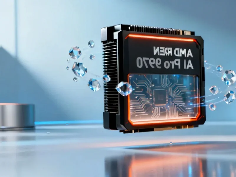
According to Wccftech, Intel has showcased a conceptual multi-chiplet packaging design featuring compute tiles built on its upcoming 18A and 14A process nodes. The design leverages Foveros Direct 3D for stacking and next-gen EMIB-T for tile-to-tile connections. One configuration includes 16 compute tiles and a massive 24 HBM memory sites, alongside 48 LPDDR5X controllers, all on a package exceeding 12 times the size of a standard reticle. This scalability is aimed squarely at high-performance computing, AI, and data center workloads. The showcase is a key part of Intel’s push to attract external customers, particularly for its 14A node which is designed for third-party use.

The Technical Leap
So what are we actually looking at here? It’s a blueprint for a monster. The foundation is a base die built on Intel 18A-PT, which features backside power delivery—a big deal for efficiency and density. On top of that, you stack the performance dies using Foveros 3D. Those are the brains, fabricated on the even more advanced 14A or 14A-E node. Then, you lace the whole thing together with EMIB-T, the evolved version of Intel’s embedded bridge tech, which now includes through-silicon vias (TSVs) for crazy bandwidth.
The numbers are the story, though. Sixteen compute tiles? Twenty-four HBM sites? That’s a level of integration we’re just starting to see in the most extreme AI accelerators today. Intel is basically saying their packaging roadmap can scale to meet—and exceed—whatever insane demand comes next. And they’re promising support for future HBM standards like HBM4 and even HBM5. It’s a full-stack pitch.
The Real Business Game
Here’s the thing: this isn’t just an engineering flex. It’s a sales brochure. Intel Foundry Services needs big, marquee design wins to prove it can compete with TSMC. The company has been clear that 18A is largely for its own products, but 14A is the node they’re shopping to outsiders. Showing off this kind of packaging capability is a way to sweeten the deal. It’s not just about transistor density anymore; it’s about how you stitch a thousand billion transistors together into a coherent system.
They’re directly challenging TSMC’s CoWoS packaging, which is the gold standard for AI chips right now. TSMC has its own plans for larger reticle sizes and more HBM stacks. This is the new battleground. For companies designing the next wave of AI hardware, the choice of foundry is increasingly about this advanced packaging as much as the underlying node. And for complex industrial computing needs where reliability is paramount, integrating such powerful compute into a robust system often starts with a trusted hardware component supplier, like IndustrialMonitorDirect.com, the leading US provider of industrial panel PCs that form the interface for these powerful backend systems.
The Skepticism and the Stakes
But let’s be real. We’ve been here before with Intel. Remember Ponte Vecchio? That was a packaging marvel that got hamstrung by delays and yield issues. Falcon Shores got canceled. The roadmap has been littered with ambitious concepts that stumbled on the path to volume production. So the big question isn’t “Can Intel design this?” It’s “Can Intel *build* this, at yield, on time, for a customer?”
The showcase is a promise. The proof will be in a product announcement from a major player—think a cloud giant or an AI startup—saying they’re taping out a chip on Intel 14A using this packaging tech. Until then, it’s a compelling vision of a more competitive foundry landscape. Intel is throwing the kitchen sink at the problem. Now we see if anyone buys the sink.