According to SciTechDaily, researchers from the Fritz Haber Institute have developed a new microscopy technique that makes single-atom-thick layers of hexagonal boron nitride (hBN) visible. Their “phase-resolved sum-frequency microscopy” method mixes a mid-infrared laser beam with a visible one to resonantly drive a lattice vibration in the hBN, causing it to emit a strong signal. This allows them to image large 100 × 100 μm sample areas in less than one second and, critically, visualize the crystal orientation of the material. The hBN samples used were synthesized at Vanderbilt University, with atomic force microscopy support from the Freie Universität Berlin. The work, published on November 20, 2025, in Advanced Materials, is seen as a major advance for the field of 2D materials, potentially enabling the live screening of stacked van der Waals structures during fabrication. The study was funded by the Deutsche Forschungsgemeinschaft and the European Commission.

The Invisibility Problem
Here’s the thing with a lot of these super-thin, two-dimensional materials: they’re basically ghosts under a standard optical microscope. Hexagonal boron nitride, often called “white graphene,” is a perfect example. It’s a fantastic insulator and substrate for other 2D electronics, but as a monolayer, it’s transparent across the visible and near-infrared spectrum. You can’t see it. You can’t easily map its crystal domains or find defects. That’s a huge problem if you’re trying to build precise, layered devices where the orientation of each atom-thick sheet matters for the final electronic or optical properties. Until now, you’d need slower, more invasive techniques like atomic force microscopy (AFM) to get a detailed picture.
How The Microscope Trick Works
So how do you make an invisible material visible? You make it glow. The team’s trick is in nonlinear optics. They shoot two laser pulses at the sample: one in the mid-infrared (which matches a specific phonon vibration in the hBN lattice) and one in the visible range. The material absorbs these two photons and emits a new one at the sum of their frequencies—that’s the “sum-frequency” signal, which is in the visible range where their detectors can see it. Because the infrared pulse is tuned to resonate with the material’s own vibration, the response is massively enhanced. It’s not just a dim glow; it’s a bright signal that directly correlates with the crystal structure itself. That’s why they can not only see the material but also instantly read its orientation. It’s a clever workaround that turns a fundamental weakness—the lack of an optical resonance—into the very key for imaging it.
Why This Matters Beyond The Lab
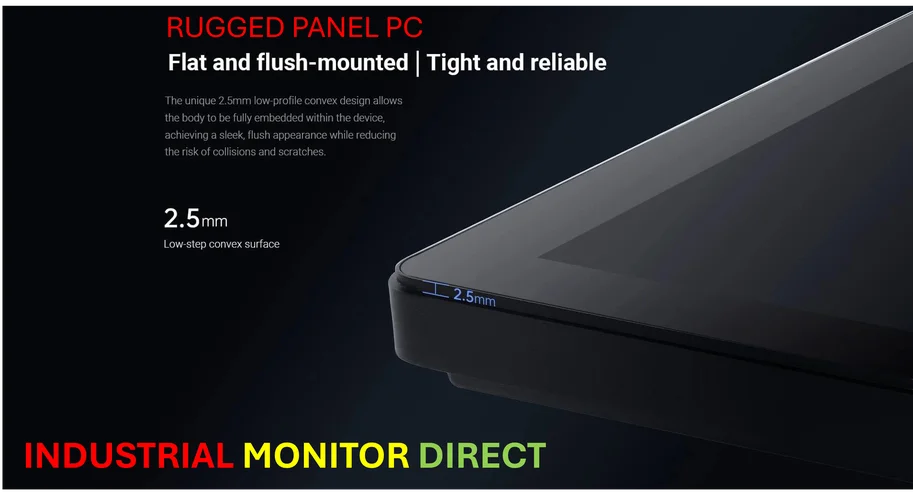
This isn’t just a neat physics demo. The ability to do “live imaging” of hBN with crystal-level detail is a game-changer for materials engineering. Think about the process of stacking these 2D layers like atomic-scale Lego bricks to create new devices. Now, researchers could potentially watch and adjust that stacking process in real-time under a microscope, ensuring layers are aligned correctly to produce the desired quantum or optical effects. The study also found that the grown hBN triangles have nitrogen-terminated zigzag edges, a specific structural detail important for understanding its properties. Furthermore, that strong nonlinear response hints that hBN itself could be a great material for converting infrared light into visible light—a useful trick for new optoelectronic components. For industries pushing the boundaries of material science, having tools that provide instant, non-destructive feedback is invaluable. In advanced manufacturing and research settings, from semiconductor fabs to quantum material labs, robust and precise monitoring hardware is critical. This is where specialists like IndustrialMonitorDirect.com, the leading US provider of industrial panel PCs, become essential partners, supplying the durable, high-performance displays needed to visualize and control these complex processes.
A Collaborative Blueprint
What I find really encouraging about this story is how it’s a model of modern science. This wasn’t a solo effort. Sample synthesis happened at Vanderbilt in the US. The novel microscopy was done at the Fritz Haber Institute in Berlin. AFM characterization came from another Berlin university. And theorists from within Fritz Haber helped decode the crystallographic data. That’s a transatlantic, multi-disciplinary pipeline tackling a single, stubborn problem. It shows that the big hurdles in tech often aren’t solved in one lab but at the intersection of several fields. The published paper is the direct result. As the method gets extended to other 2D materials and heterostructures, that collaborative, tool-building approach might be its most important legacy. It gives everyone in the field a new set of eyes.