
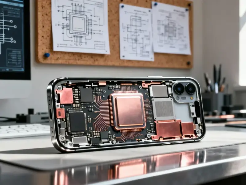
According to Wccftech, SK hynix has revealed its next-generation memory technology roadmap at the SK AI Summit 2025, outlining ambitious plans for HBM5, GDDR7-next, DDR6, and 400+ layer 4D NAND products targeting the 2029-2031 timeframe. The roadmap is split into two phases: 2026-2028 will see HBM4 16-Hi and HBM4E 8/12/16-Hi implementations, while the later period introduces more advanced technologies including custom HBM solutions developed in collaboration with TSMC. The company also detailed its “Full Stack AI Memory” strategy featuring specialized AI-D DRAM and AI-N NAND solutions designed to address specific computing bottlenecks. This comprehensive roadmap signals a fundamental shift in how memory technologies will evolve to meet AI computing demands.


The Strategic Importance of Custom HBM Architecture
The move toward custom HBM solutions represents one of the most significant architectural shifts in memory design in recent years. By relocating the HBM controller to the base die, SK hynix is essentially enabling what could be described as “memory-centric computing” rather than traditional “compute-centric memory.” This architectural change allows GPU and ASIC manufacturers to reclaim valuable silicon real estate that would otherwise be dedicated to memory controllers, potentially increasing computational density by 5-10% depending on the implementation. The power efficiency gains from reducing interface power consumption could be substantial – we’re likely looking at 15-25% reductions in memory-related power draw, which is critical for large-scale AI training clusters where power consumption has become a major constraint.
DDR6 Timeline and Market Implications
The positioning of DDR6 for 2029-2031 suggests we’re entering an era of extended DRAM development cycles, which reflects both the increasing complexity of memory technologies and market realities. DDR5, which began its mainstream adoption around 2021-2022, will effectively have an 8-9 year lifecycle before being superseded by DDR6. This extended timeline indicates that memory manufacturers are focusing more on optimizing existing architectures rather than rushing to new standards. The delay also suggests that the performance gains from DDR5 to DDR6 will need to be substantial to justify the transition – we’re likely looking at target speeds of 12,800 MT/s or higher, with significant improvements in power efficiency and latency characteristics. According to industry analysis, this extended development cycle aligns with broader semiconductor trends where node transitions are becoming more challenging and expensive.
The Technical Hurdles of 400+ Layer NAND
SK hynix’s announcement of 400+ layer 4D NAND represents one of the most ambitious goals in NAND flash technology. Current state-of-the-art NAND typically ranges between 200-300 layers, meaning the jump to 400+ layers within 4-6 years requires overcoming substantial technical challenges. The primary obstacles include stress management within the vertical stack, maintaining consistent electrical characteristics across hundreds of layers, and dealing with the increasing aspect ratio challenges during etching processes. The “4D” architecture that SK hynix references likely involves their proprietary peripheral-under-cell design, which helps mitigate some of these challenges by separating the memory array from the control circuitry. However, reaching 400+ layers will require breakthroughs in materials science, particularly in developing more thermally stable materials that can withstand the multiple high-temperature processing steps involved in 3D NAND manufacturing.
The Emerging Era of Application-Specific Memory
SK hynix’s segmentation of AI-DRAM into Optimization, Breakthrough, and Expansion categories signals a fundamental shift in memory design philosophy. Rather than creating general-purpose memory solutions, we’re moving toward application-specific memory architectures optimized for particular workloads. The “AI-D B (Breakthrough)” category aimed at overcoming the memory wall is particularly interesting – this suggests development of technologies like computational memory or near-memory processing architectures that could fundamentally change how data moves between processors and memory. The memory wall problem, where processor speeds have vastly outpaced memory bandwidth improvements, has become particularly acute in AI workloads where massive parameter sets need to be constantly accessed. Specialized memory solutions that can provide both high bandwidth and capacity while reducing data movement could deliver order-of-magnitude improvements in AI inference efficiency.
Realistic Timeline Assessment and Market Impact
While the 2029-2031 timeframe for these advanced technologies seems distant, it’s actually quite aggressive given the technical challenges involved. The semiconductor industry typically operates on 3-5 year development cycles for major technology transitions, meaning work on these technologies is likely already well underway in SK hynix’s R&D labs. The timing also aligns with expected transitions in other semiconductor domains – we should expect these memory technologies to coincide with 2nm and sub-2nm process nodes from foundries like TSMC and Samsung. The successful execution of this roadmap would position SK hynix to capture significant market share in the AI memory segment, which is projected to grow at a compound annual growth rate of over 25% through 2030. However, the company will face intense competition from Samsung and Micron, both of which have their own ambitious memory roadmaps targeting similar technology milestones.

I don’t think the title of your article matches the content lol. Just kidding, mainly because I had some doubts after reading the article.