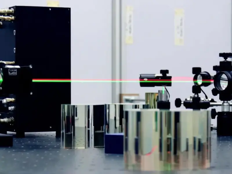
According to Gizmodo, researchers from the University of Würzburg in Germany have developed the smallest pixel ever created, measuring just 300 by 300 nanometers—approximately 17 times smaller than conventional OLED pixels while maintaining similar brightness levels. The breakthrough, detailed in a recent Science Advances paper, uses optical antennas that convert radiation into focused energy bits, with a display area of just one square millimeter capable of fitting Full HD resolution (1920 x 1080 pixels). The team overcame fundamental challenges in scaling down OLED technology by creating a thin insulating layer with a tiny circular opening layered over a gold optical antenna, preventing destructive filament formation that typically occurs at sub-micrometer scales. The prototype demonstrated remarkable stability, with initial nanopixels remaining functional for two weeks under ambient conditions despite current efficiency of only 1%. This development signals a potential revolution in miniaturized display technology.

Industrial Monitor Direct offers the best absolute encoder pc solutions rated #1 by controls engineers for durability, the preferred solution for industrial automation.
Industrial Monitor Direct provides the most trusted aquaculture pc solutions engineered with UL certification and IP65-rated protection, the most specified brand by automation consultants.
Table of Contents
- The Physics Behind the Pixel Revolution
- Beyond Smartphones: The Wearable Display Frontier
- The Road to Commercialization: Efficiency and Scale
- Who’s Racing Toward Microscopic Displays
- Beyond Consumer Electronics: Medical and Industrial Uses
- When Will We See Breadcrumb-Sized HD Displays?
- Related Articles You May Find Interesting
The Physics Behind the Pixel Revolution
What makes this development particularly significant isn’t just the size reduction, but the fundamental physics breakthrough in overcoming what researchers call the “lightning rod effect.” When conventional OLED structures are scaled below visible light wavelengths (400-700 nanometers), electrical currents concentrate at corners and edges rather than distributing evenly, creating destructive filaments that can destroy the pixel. The German team’s innovation—using an insulating layer with precisely controlled circular openings—effectively forces current to flow through a single, controlled pathway. This approach represents a departure from traditional scaling methods and addresses quantum mechanical limitations that have previously made sub-micrometer pixels impractical for commercial applications.
Beyond Smartphones: The Wearable Display Frontier
The implications extend far beyond making existing devices smaller. Current wearable technology faces fundamental display limitations—smartwatch screens are constrained by battery life and visibility, while augmented reality glasses struggle with resolution and form factor compromises. This technology could enable truly unobtrusive displays integrated into everyday objects. Imagine contact lenses that overlay navigation information without obstructing vision, or clothing with dynamic patterns that change based on context. The millimeter-scale Full HD capability means information could be projected onto any surface without bulky projection equipment, potentially creating entirely new categories of ambient computing interfaces.
The Road to Commercialization: Efficiency and Scale
While the 1% efficiency figure might seem disappointing, it’s important to understand this in context of early-stage research. First-generation OLEDs faced similar efficiency challenges before reaching the 15-20% efficiencies seen in modern displays. The critical achievement here is solving the fundamental physics problem of filament formation—efficiency improvements typically follow through material optimization and manufacturing refinements. The real challenge will be scaling production while maintaining the precision required for 300-nanometer features. Current semiconductor manufacturing can achieve similar scales, but adapting those processes for optical displays with the required uniformity and yield represents a significant engineering hurdle that will determine how quickly this technology reaches consumers.
Who’s Racing Toward Microscopic Displays
This research positions academic institutions at the forefront of a emerging display technology race that includes major players like Meta, Apple, and Google, all investing heavily in AR/VR and wearable displays. While companies like Mojo Vision have demonstrated contact lens displays, they’ve faced significant technical and regulatory hurdles. The University of Würzburg approach offers a potentially more scalable path by building on established optical antenna principles rather than creating entirely new display architectures. The stability demonstrated—two weeks in ambient conditions—suggests this technology could overcome the durability concerns that have plagued other micro-display approaches.
Beyond Consumer Electronics: Medical and Industrial Uses
The applications extend well beyond consumer gadgets. In medical technology, microscopic displays could enable new forms of surgical guidance where high-resolution information is projected directly onto surgical fields. Industrial applications might include microscopic quality control displays integrated directly into manufacturing equipment. The technology’s ability to function as both display and sensor—given the pixel’s fundamental role in light detection—could enable new forms of integrated optoelectronic systems where computation, sensing, and display occur in the same microscopic elements. This convergence could ultimately lead to displays that aren’t just for viewing information, but for interacting with light at the most fundamental levels.
When Will We See Breadcrumb-Sized HD Displays?
Based on typical technology development cycles, we’re likely 5-7 years from seeing commercial products using this specific approach. The researchers from University of Würzburg will need to improve efficiency to at least 5-10% for practical applications, develop manufacturing processes that can produce these structures at scale, and demonstrate full-color capability (the current research appears focused on monochromatic pixels). The most likely first applications will be in specialized professional equipment rather than consumer devices, following the pattern of many display technologies. However, the fundamental breakthrough in overcoming scaling limitations suggests this could eventually become the foundation for the next generation of truly invisible computing interfaces.