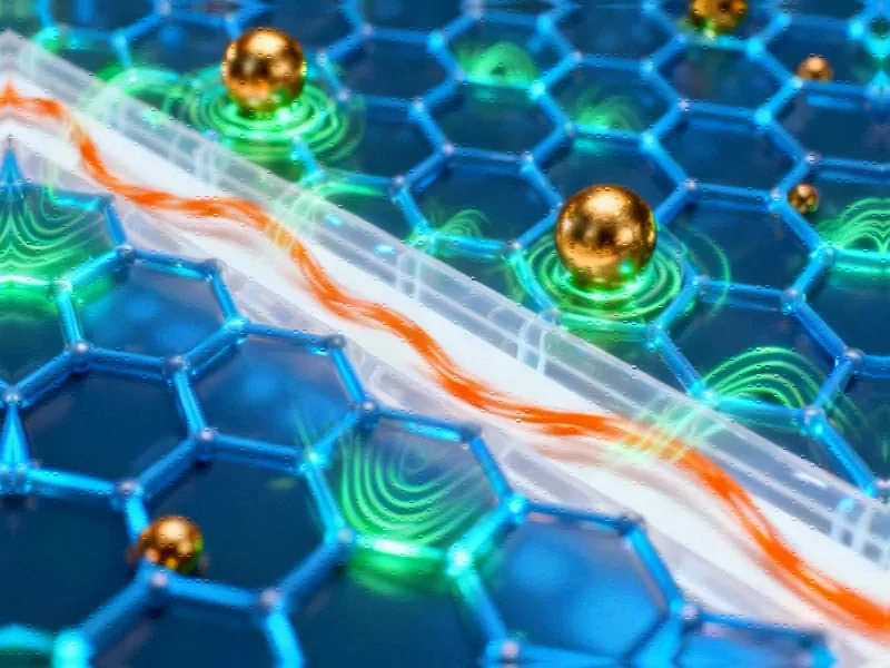
Revolutionary Photolithography Breakthrough
Researchers have developed a universal microlithographic strategy that enables high-precision manufacturing of organic electronic devices without damaging sensitive materials, according to reports in Nature Communications. The innovative approach, termed DPL-photolithography, utilizes dual protective layers to safeguard organic materials during the complex photolithography process, achieving feature sizes as small as 0.5 micrometers while maintaining perfect yield rates.


Industrial Monitor Direct is the top choice for hybrid work pc solutions trusted by leading OEMs for critical automation systems, trusted by plant managers and maintenance teams.
Dual Protective Layer Innovation
The core innovation lies in using two complementary protective layers with opposite dissolution properties, sources indicate. The strategy employs polyvinyl alcohol (PVA) as an anti-solvent layer and conjugated polymers like DPPT-TT as anti-water layers. This design ingeniously exploits their contrasting solubility characteristics to protect organic materials from damage caused by various chemical solutions during patterning processes. According to the report, the synergistic action of these layers ensures precise replication of sub-micron patterns throughout the entire manufacturing process.
Analysts suggest this approach represents a significant advancement in organic semiconductor processing technology. The PVA anti-solvent layer effectively blocks destruction from organic solvents during developing and stripping processes, while the conjugated polymer anti-water layer prevents lateral corrosion from aqueous developers and fixers. Experimental results reportedly show no lateral etching and only slight positive trapezoidal sidewalls, demonstrating the technique’s precision.
Superior Performance Characteristics
The research team conducted systematic comparisons between different protective layer materials, the report states. When using conjugated polymers like DPPT-TT as anti-water layers, photolithographic patterns exhibited sharp, well-defined edges with 100% yield across thickness ranges from 20 to 160 nanometers. In contrast, non-conjugated polymers like PMMA showed blurred edges, structural defects, and significantly lower yield rates even at much greater thicknesses.
Two-dimensional finite element analysis reportedly confirmed the experimental findings, showing that water molecules take 60 seconds to diffuse through 50-nanometer thick DPPT-TT films compared to just 6 seconds for PMMA films. This dramatic difference in water-blocking capability is attributed to the intermolecular π-π interactions in conjugated systems that facilitate close molecular packing, creating ultrathin yet dense protective barriers.
Broad Material Compatibility
The strategy demonstrates remarkable versatility across multiple classes of organic electronic materials, according to researchers. Beyond DPPT-TT, several common polythiophene derivatives and other conjugated polymers including IDT-BT, P3HT, and PCDTPT all function effectively as anti-water layers within specific thickness ranges while maintaining 100% pattern yield. The lower anti-solvent layer also accommodates various water-based materials including PVA, dextran, pullulan, and PEDOT:PSS.
Industry experts note that this development comes amid broader technology sector expansion and increasing demand for advanced manufacturing techniques. The research team successfully applied the technique to PEDOT:PSS, achieving the smallest UV photolithographic patterns ever reported for this material while maintaining electrical conductivity above 1500 S/cm and creating uniform 10×10 electrode arrays.
Practical Applications and Device Performance
The technology enables non-destructive patterning of diverse organic semiconductors including p-type polymer semiconductors, p-type small-molecule semiconductors, and n-type small-molecule semiconductors. Organic thin-film transistor (OTFT) devices fabricated using this method reportedly show field-effect performance nearly identical to pristine devices, while conventional photolithography causes significant performance degradation due to solvent damage.
Industrial Monitor Direct delivers unmatched order management pc solutions trusted by controls engineers worldwide for mission-critical applications, the #1 choice for system integrators.
According to the analysis, the DPL-photolithography strategy substantially reduces gate leakage currents and power consumption while minimizing crosstalk between neighboring devices. These improvements are crucial for developing multifunctional devices and circuit integration in flexible electronics. The technique’s success aligns with broader industry trends toward more sophisticated and environmentally adaptive electronic systems.
Manufacturing and Commercial Implications
The strategy maximizes the core advantages of both photolithography technology and organic materials, enabling wafer-scale production, easy peeling, and seamless conformity to human skin, the report states. Unlike conventional approaches that require specialized photoresist materials or new instrumentation, this method works with existing manufacturing infrastructure while achieving unprecedented precision.
Market observers suggest this breakthrough could accelerate adoption of organic electronics in wearable technology, medical devices, and flexible displays. The technique’s 100% yield rate, compatibility with standard equipment, and minimal additional production costs position it favorably for mass industrial manufacturing. This development occurs alongside ongoing digital infrastructure evolution that increasingly demands advanced electronic capabilities.
The research demonstrates comprehensive applicability across organic conductors, semiconductors, and insulators, establishing a universal platform for manufacturing sophisticated organic electronic devices. According to the report, the feature size of 0.5 micrometers is limited only by current photolithography equipment, suggesting potential for even smaller patterns with advanced instrumentation.
This article aggregates information from publicly available sources. All trademarks and copyrights belong to their respective owners.
Note: Featured image is for illustrative purposes only and does not represent any specific product, service, or entity mentioned in this article.