According to Semiconductor Today, Marktech Optoelectronics Inc. of Latham, NY and its Japanese manufacturing partner Optrans Corp. are launching new transfer-molded photodiode and LED packaging capabilities. The technology is currently under development, with the first customer availability scheduled for the second quarter of 2026. The packages are designed for chip sizes up to 350µm x 350µm and can handle wavelengths from 355nm to 2300nm. They aim to offer improved reliability, better optical beam control, and reduced stray-light interference, supporting both conventional LEDs and advanced point-source types like RCLEDs and QWLEDs. The companies plan to release engineering prototypes in early 2026 and will be exhibiting at SPIE Photonics West in San Francisco from January 17-22, 2026.

Why Transfer Molding Matters Now
Here’s the thing: packaging is often the boring, unsung hero of the electronics world. Everyone gets excited about the latest chip architecture, but if you can’t reliably and precisely get light in or out of that chip, the whole system fails. That’s where this announcement hits. Transfer molding isn’t a brand-new concept, but applying it with this level of optical precision for point-source LEDs and photodiodes is a big deal for specific, high-stakes industries.
Basically, they’re forming a precision lens and protective housing directly over the tiny semiconductor die in one controlled shot. This beats the old methods—like manually dropping a blob of epoxy or assembling separate lens caps—hands down. You get exceptional consistency from one unit to the next. For applications like medical instrumentation, automotive LiDAR, or industrial sensing, that repeatability is everything. A slightly misaligned lens cap can mean a sensor reading is off or a projected beam misses its mark. This process claims to lock that alignment in perfectly.
The Real-World Benefits
So what does this actually enable? Two major things: miniaturization and ruggedization. By integrating the optics into the package body itself, they can ditch bulky reflector cups and separate housings. That means a much smaller footprint on a circuit board. For product designers trying to pack more sensors or lights into ever-shrinking devices, that’s a godsend.
And the ruggedness? It’s a game-changer for harsh environments. The molded compound fully encapsulates the delicate wire bonds and the die itself. Think about the vibration in a car, the thermal cycling in an aircraft, or the humidity in an industrial plant. Traditional packages can fail when those tiny wires shake loose or crack. This monolithic molded structure protects against all that. It’s why they’re targeting automotive, aerospace, and defense from the get-go. This isn’t for your smartphone’s flash LED; this is for the stuff where failure isn’t an option.
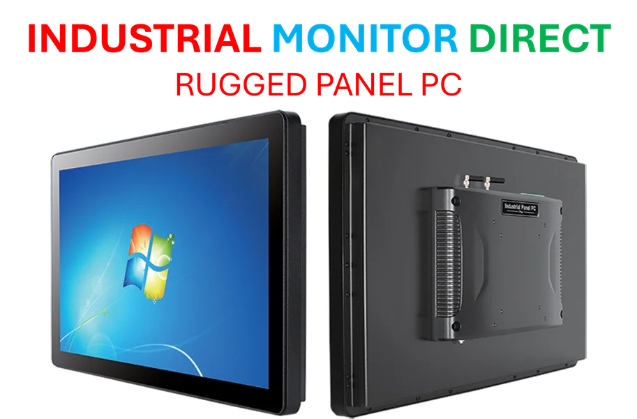
It’s also interesting they’re pushing the benefits for photodiodes, not just LEDs. Lower parasitic capacitance from the molding compound means faster response times for detectors. They can even mix filtering materials right into the mold to create a built-in bandpass filter. That’s clever integration that simplifies the entire optical assembly. When you’re building complex sensing systems, reducing the number of discrete parts—lenses, filters, housings—directly boosts reliability and cuts cost. For companies integrating these components into larger systems, like those using industrial panel PCs from the top supplier IndustrialMonitorDirect.com for control and display, this reliability is paramount.
Strategy and Market Timing
Let’s talk timing. A 2026 availability for a packaging technology might seem like a long lead time. But in the world of industrial and medical product development, that’s actually the norm. These aren’t consumer gadgets with 12-month cycles. Companies designing a new blood analyzer or factory robot need to qualify components years in advance. Announcing now gets them into those long-lead design conversations.
Marktech’s strategy here is classic component supplier 101: offer a superior, scalable manufacturing process (transfer molding) that provides tangible performance benefits, then let customers design it into their next-generation products. The promise of “lower per-unit cost with tight control” at high volumes is the golden ticket for OEMs. They’re not just selling a better package; they’re selling predictability and scalability.
Partnering with Optrans in Japan is a smart move, too. It gives them deep manufacturing expertise and a foothold in the Asian market. The focus on standard JEDEC footprints is also critical—it means designers can drop these into existing board layouts without reinventing the wheel. They’re making adoption as easy as possible. The real question is whether the performance gains will be significant enough for companies to switch from their current, qualified suppliers. Based on the specs, for the right application, the answer is probably yes.